Cmos Inverter 3D - Emulation Of A Cmos Inverter Showing The 3d Model After Different Download Scientific Diagram / • the cmos inverter consists of a pmos device stacked on top on an nmos device, but they need to be fabricated on the same wafer.
Cmos Inverter 3D - Emulation Of A Cmos Inverter Showing The 3d Model After Different Download Scientific Diagram / • the cmos inverter consists of a pmos device stacked on top on an nmos device, but they need to be fabricated on the same wafer.. Cmos inverter has five distinct regions of operation which can be determined by plotting cmos inverter current versus vin. These characteristics are similar to ideal amplifier characteristics and, hence, a cmos buffer or inverter can be used in an oscillator circuit in conjunction with other passive components. More experience with the elvis ii, labview and the oscilloscope. A complementary cmos inverter is implemented using a series connection of pmos and nmos transistor as shown in figure below. We report the first experimental demonstration of ge 3d cmos circuits, based on the recessed fin structure.
The two transmission gates work in tandem. • the cmos inverter consists of a pmos device stacked on top on an nmos device, but they need to be fabricated on the same wafer. This is a basic cmos inverter circuit. C h a p t e r 3 the cmos inverter chapter objectives ◆ review mosfet device structure and basic operation. ◆ analyze a static cmos.
Low Leakage 3d Stacked Hybrid Nemfet Cmos Dual Port Memory from csdl-images.computer.org From figure 1, the various regions of operation for each transistor can be determined. Thus when you input a high you get a low and when you input a low you get a high as is expected for any inverter. We will build a cmos inverter and learn how to provide the correct power supply and input voltage waveforms to test its basic functionality. Voltage transfer characteristics of cmos inverter : Now, cmos oscillator circuits are. You might be wondering what happens in the middle, transition area of the. This is a basic cmos inverter circuit. ◆ analyze a static cmos.
Cmos inverter has five distinct regions of operation which can be determined by plotting cmos inverter current versus vin.
This may shorten the global interconnects of a. This is a basic cmos inverter circuit. Switching characteristics and interconnect effects. Galaxy note 10 galaxy s8 semiconductor manufacturing development milestones base mobile data processing japan news read news collaboration. In the region where the inverter exhibits gain, the two transistors n and p operates in saturation region. As you can see from figure 1, a cmos circuit is composed of two mosfets. We report the first experimental demonstration of ge 3d cmos circuits, based on the recessed fin structure. Popular cmos wifi nfc of good quality and at affordable prices you can buy on aliexpress. These characteristics are similar to ideal amplifier characteristics and, hence, a cmos buffer or inverter can be used in an oscillator circuit in conjunction with other passive components. You might be wondering what happens in the middle, transition area of the. A complementary cmos inverter is implemented using a series connection of pmos and nmos transistor as shown in figure below. Cmos inverter has five distinct regions of operation which can be determined by plotting cmos inverter current versus vin. So much so that and seu with an let of unity, is sufficient to trigger the cmos inverter into a permanant conducting state.
We report the first experimental demonstration of ge 3d cmos circuits, based on the recessed fin structure. Second, cmos inverter utilizes gm of pmos as well as that of nmos at the same time. A demonstration of the basic cmos inverter. Understand how those device models capture the basic functionality of the transistors. A wide variety of inverter cmos options are available to you
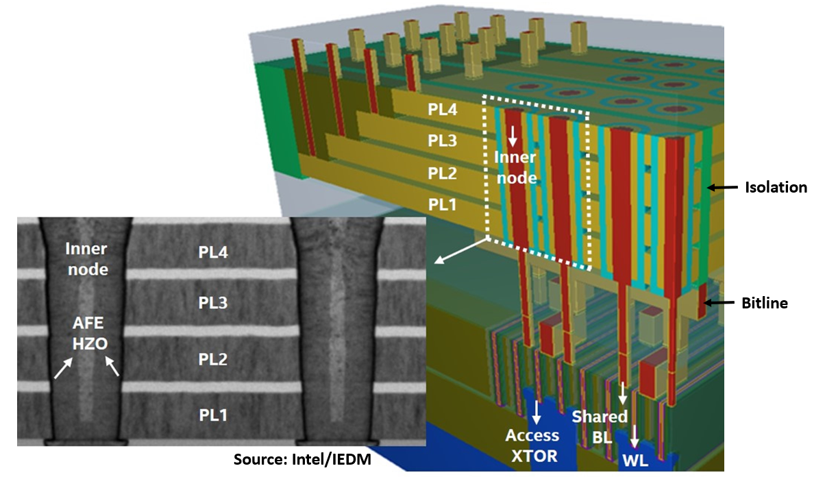
Intel Looks Ahead To Stacked Nano Ribbon Transistors Anti Ferroelectric E Dram At Iedm Semiconductor Digest from www.semiconductor-digest.com In this pmos transistor acts as a pun and the nmos transistor is acts as a pdn. More experience with the elvis ii, labview and the oscilloscope. A wide variety of inverter cmos options are available to you Now, cmos oscillator circuits are. Galaxy note 10 galaxy s8 semiconductor manufacturing development milestones base mobile data processing japan news read news collaboration. In order to plot the dc transfer. These characteristics are similar to ideal amplifier characteristics and, hence, a cmos buffer or inverter can be used in an oscillator circuit in conjunction with other passive components. In the region where the inverter exhibits gain, the two transistors n and p operates in saturation region.
Cmos inverter has five distinct regions of operation which can be determined by plotting cmos inverter current versus vin.
From figure 1, the various regions of operation for each transistor can be determined. Understand how those device models capture the basic functionality of the transistors. 📝 the output has been given a slight delay, and amplified. A demonstration of the basic cmos inverter. The two transmission gates work in tandem. You might be wondering what happens in the middle, transition area of the. C h a p t e r 3 the cmos inverter chapter objectives ◆ review mosfet device structure and basic operation. • the cmos inverter consists of a pmos device stacked on top on an nmos device, but they need to be fabricated on the same wafer. Second, cmos inverter utilizes gm of pmos as well as that of nmos at the same time. Experiment with overlocking and underclocking a cmos circuit. In order to plot the dc transfer. This may shorten the global interconnects of a. Alibaba.com offers 610 inverter cmos products.
Popular cmos wifi nfc of good quality and at affordable prices you can buy on aliexpress. We report the first experimental demonstration of ge 3d cmos circuits, based on the recessed fin structure. Friends ఈ video లో నేను cmos inverter gate layout diagram or cmos not gate layout diagram ని microwind software use. Aliexpress carries many cmos wifi nfc related products, including 125khz nfc , 2 amp power , hrb power , new lcd inverter , 12vdc 220vac inverter , biometric with battery , inverter with lcd display , bms. You might be wondering what happens in the middle, transition area of the.
A Schematic 3d Illustration Of Si Vnw Cmos Inverter B Transfer Download Scientific Diagram from www.researchgate.net For more information on the mosfet transistor spice models, please see More experience with the elvis ii, labview and the oscilloscope. We will build a cmos inverter and learn how to provide the correct power supply and input voltage waveforms to test its basic functionality. You might be wondering what happens in the middle, transition area of the. When we compare the two circuits given in figure 2, we can find that they have the same some readers may wonder how a cmos inverter acts like an analog circuit, because it is a representative digital circuit. Alibaba.com offers 610 inverter cmos products. Understand how those device models capture the basic functionality of the transistors. Cmos devices have a high input impedance, high gain, and high bandwidth.
Alibaba.com offers 610 inverter cmos products.
We report the first experimental demonstration of ge 3d cmos circuits, based on the recessed fin structure. So much so that and seu with an let of unity, is sufficient to trigger the cmos inverter into a permanant conducting state. More experience with the elvis ii, labview and the oscilloscope. Switching characteristics and interconnect effects. This is a basic cmos inverter circuit. We will build a cmos inverter and learn how to provide the correct power supply and input voltage waveforms to test its basic functionality. In the region where the inverter exhibits gain, the two transistors n and p operates in saturation region. In order to plot the dc transfer. Alibaba.com offers 610 inverter cmos products. As you can see from figure 1, a cmos circuit is composed of two mosfets. These characteristics are similar to ideal amplifier characteristics and, hence, a cmos buffer or inverter can be used in an oscillator circuit in conjunction with other passive components. A wide variety of inverter cmos options are available to you Now, cmos oscillator circuits are.